Photonics, Optics and Quantum Shine in Capital Region Semiconductor Patents
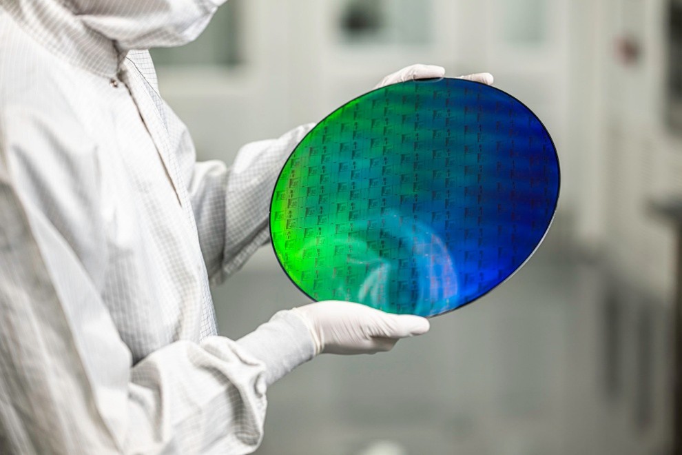
A quantum photonic chipset. Courtesy PsiQuantum
Highlights
- In 2025, the USPTO awarded nearly 600 semiconductor-related patents that list Capital Region inventors.
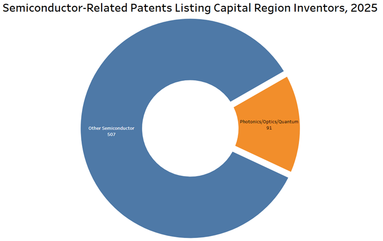
- 1 in 6 semiconductor patents listing local inventors pertained to photonics, optics, and/or quantum computing.
- GlobalFoundries is positioned to accelerate photonics R&D under $300 million agreement with U.S. Department of Commerce.
- PsiQuantum and Quantinuum source quantum computing components from GF.
- Capital Region job postings for photonics engineers spiked in 2025.
The Capital Region’s R&D industry is shining brighter, with one out of six of the semiconductor-related patents that were awarded in 2025 and that listed local inventors involving photonics, optics and/or quantum computing, according to a Center for Economic Growth analysis of data from the U.S. Patent and Trademark Office (USPTO).
Patents
From NY Creates and the AIM Photonics Manufacturing Innovation Institute to PsiQuantum and GlobalFoundries, Capital Region researchers are developing new light-based technologies that are more energy efficient and faster than their electron-based counterparts. These photonic innovations are critical for next-generation artificial intelligence datacenters, quantum computing, and automotive and aerospace/defense applications with increasing bandwidth and power pressures.
In 2025, the USPTO awarded about 600 semiconductor-related patents1 listing inventors who live in the Capital Region. Among them, 91, or 14 percent, had Cooperative Patent Classification (CPC) codes relating to silicon photonics/optics2 and/or quantum computing3. That means almost one in six semiconductor patents listing local inventors pertain to those fields.
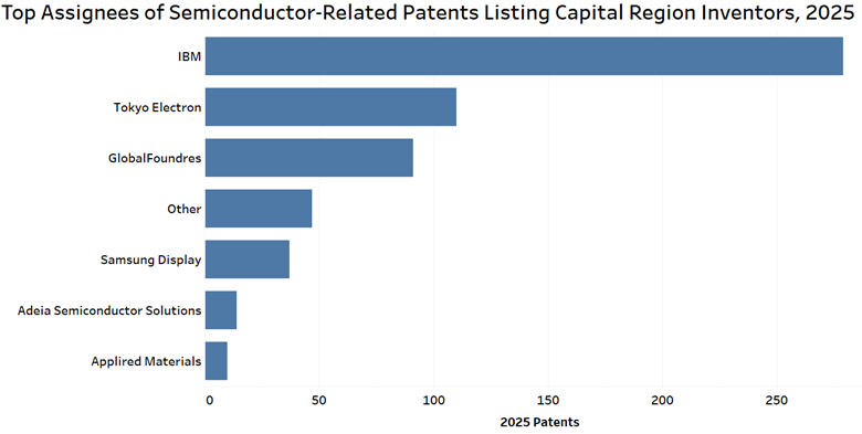
Nearly half of those photonics/optics/quantum-related patents (48 percent) were assigned to GF and nearly one-fifth (19 percent) were assigned to Tokyo Electron, which operates a research center at NY Creates’ Albany NanoTech Complex. Other assignees included PsiQuantum, Rensselaer Polytechnic Institute, NY Creates (with researchers assigned to AIM Photonics), and IBM. While IBM is planning to build the nation’s first quantum foundry at Creates’ Albany NanoTech Complex, its core quantum R&D hub is at its Yorktown Heights research center in the Hudson Valley.
GlobalFoundries
With GF last month entering a $300 million agreement with the U.S. Department of Commerce to accelerate silicon photonics R&D, the region is positioned to generate more patents for photonic and optical technologies. More specifically, GF stated it will focus on R&D for next-generation silicon photonics wafer technologies, and novel optical materials. GF will also pursue R&D for advanced packaging to support the launch of near-packaged optics (NPO) and co-packaged optics (CPO). This R&D will build off GF’s recently introduced Silicon Photonics Co-Packaged Advanced Light Engine (SCALE) platform.
“We are pleased to take a central role in advancing optical innovation and development in the U.S. and believe this recognition validates the strategic importance of silicon photonics, the excellent relationship we enjoy with our partners and GF leadership in these technologies,” GF CEO Timothy Breen said in a recent Q2 2026 earnings call. He noted that GF’s silicon photonics revenues are on track to be more than double in 2026 when compared to the previous year.
GF’s domestic silicon photonics production was initially based at Fab 10 in East Fishkill, which the company acquired from IBM in 2015. In 2022, GF – with $117 million in funding from the Department of Defense – transferred Fab 10’s monolithic 45 nm silicon-on-insulator (SOI) platform to Fab 8. That same year, GF announced the launch of its monolithic 45 nm SOI CMOS-silicon photonics platform, called Fotonix.
AIM Photonics
Years before GF started Fotonix manufacturing in Malta, photonics R&D was already underway in the Capital Region. In 2015, the Department of Defense (now the Department of War), announced the nation’s first US-based institute for manufacturing integrated photonics: the American Institute for Manufacturing Integrated Photonics (AIM Photonics), a $600-million-plus initiative for silicon photonics prototyping. In 2021, DoD awarded a $321 million, seven-year extension that, with 50 percent matching funds from New York State and other sources, further enabled the AIM Photonics Institute at NY Creates, which operates an open-access 300 mm silicon photonics prototyping and multi-project wafer (MPW) platform to likewise undertake test, assembly, and packaging operations.
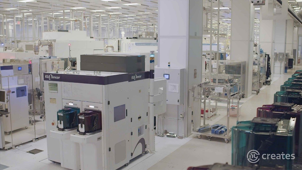
A cleanroom in NY Creates’ Albany NanoTech Complex. Courtesy NY Creates.
“AIM Photonics is positioned to address three of the six critical defense technologies areas of quantum information dominance, applied AI, and biomanufacturing creating both global competitiveness and economic growth for the U.S. and New York State where the institute operates,” said AIM Photonics Executive Director Nicholas Fahrenkopf. “In addition, chips developed at AIM Photonics were recently chosen to study the effects of harsh environments for space-qualified photonic applications on board the International Space Station.”
Last month, AIM Photonics introduced an assembly design kit to streamline photonic package design, and is currently offering its first Quantum Flex MPW run accelerating the photonics community’s adoption of quantum applications.
PsiQuantum/Quantinuum
In 2019, PsiQuantum in Palo Alto, California established a relationship with GlobalFoundries, and two years later they publicly announced a major breakthrough in their partnership. That 2021 breakthrough centered on the manufacturing of silicon photonic and electronic chips for PsiQuantum’s Q1 system that served as the initial intermediate step toward the world’s full-scale quantum computer, for which silicon photonics is foundational. In 2022, PsiQuantum began to move from Fab 10 in East Fishkill to Fab 8 in Malta, following GF’s transfer of the 45 nm SOI platform for its silicon photonics chips.
In 2023, NY Creates also partnered with PsiQuantum for integrated photonics R&D to advance quantum technology solutions. Last February, PsiQuantum announced the development of a quantum photonic chipset purpose-built for utility-scale quantum computing. The chipset, dubbed “Omega”, is made at GF’s Fab 8 in Malta. In June, PsiQuantum broke ground on what will be the world’s first utility-scale quantum computer in Australia.
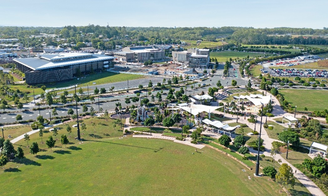
PsiQuantum is building the world’s first utility-scale quantum computer at Moreton Bay Central in Queensland, Australia. GF Fab 8 in Malta has made thousands of silicon photonic wafers designed by PsiQuantum.
In May, GF launched Quantum Technology Solutions, a new business unit dedicated to scaling the manufacturing capabilities for utility-scale quantum computing. GF identified both PsiQuantum and Quantinuum in Broomfield, Colorado as partners in the Quantum Technology Solutions initiative.
In May, Quantinuum also entered an agreement with the Commerce Department, which will provide funding for quantum computing-related R&D. Quantinuum pledged to partner with GF for critical semiconductor components. Quantinuum’s president and CEO, Rajeeb Hazra credited GF with helping his company’s efforts to scale ion trap quantum computing “by combining cryogenic CMOS, integrated photonics and advanced packaging in a secure U.S. manufacturing environment.” Cryogenic CMOS is made on GF’s FDX fully depleted silicon-on-insulator (FD-SOI) platform, which was introduced to Fab 8 around 2024.
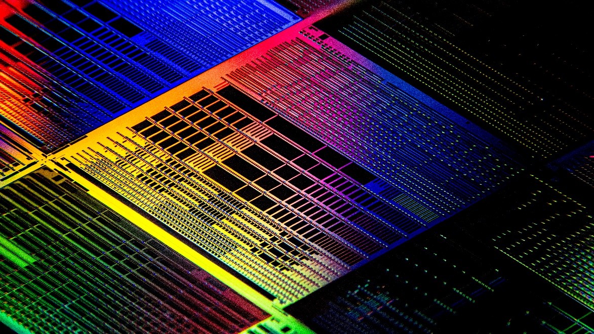
A quantum photonic chip. Courtesy PsiQuantum
Photonics Engineers
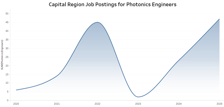
Demand for photonics engineers has been increasing since GF’s rollout of its silicon photonics chips at Fab 8 in 2022. That year, the number of Capital Region unique job postings for photonics engineers increased to 45, compared to 14 the previous year. Photonics engineer job postings spiked again in 2025 at 47, with openings at NY Creates in Albany and GF and Quantinuum in Malta, according to jobs posting data from Lightcast.
In 2025, GF announced it will develop in Malta a $575 million New York Advanced Packaging and Photonics Center that will employ 100 over five years. On top of that was a $186 million investment in R&D over the next decade. Later that year, GF pledged an additional $3 billion for R&D initiatives involving advanced packaging, silicon photonics and next-generation gallium nitride (GaN) technologies.
Notes
USPTO data for annual patent awards by assignee from Open Data Portal’s PatentsView Annualized Patent Data. The patent numbers from this dataset were matched with those from USPTO Patent Public Search data for 2025 (PY.), which was limited to Capital Region towns and cities (INCI. and INST.). Assisted by Grok (xAI) in identifying relevant CPC classifications for semiconductor-related and photonic/optic/quantum technologies, August 2026.
1 Semiconductor-related patent CPC codes: B01D, B82B 3/00, B82Y 10/00, B82Y 20/00, C23C, C30B, G02B, G02B 5/00, G02F, G03F 1/00, G03F 7/00, G05B 13/00, G06N 10/00, G11C, H01J 37/00, H01L, H01S 5/00, H04B 10/70, H04L 9/085, H05K, H10,
2 Silicon photonics/optics-related patent CPC codes: B82Y 20/00, G02B 6/00, G02F 1/00, G03F 7/00, H01S 5/026, H01S 5/10, H10F 30/00, H10F 39/00, H10H 20/00
3 Quantum computing-related patent CPC codes: B82Y 10/00, B82Y 20/00, G06N 10/00, H01S 5/00, H10D 30/00, H10F 30/00, H10N 60/00, H10N 69/00
CEG Initiatives
CEG has a long history of supporting the Capital Region’s semiconductor industry, from marketing the region and hosting events at SEMICON West to sponsoring several apprenticeship programs for GlobalFoundries and NY Creates to conducting a microelectronics workforce needs assessment for the Northeast Regional Defense Technology Hub (NORDTECH). CEG has also launched a Semiconductor Growth Access Program (SGAP) to strengthen the region’s semiconductor supply chain by providing targeted businesses with funding for legal, financial, business planning, and technical accounting assistance.
Don’t miss these insights into the trends that are shaping the Capital Region’s economy. Sign up for CEG’s e-news and follow us on: